
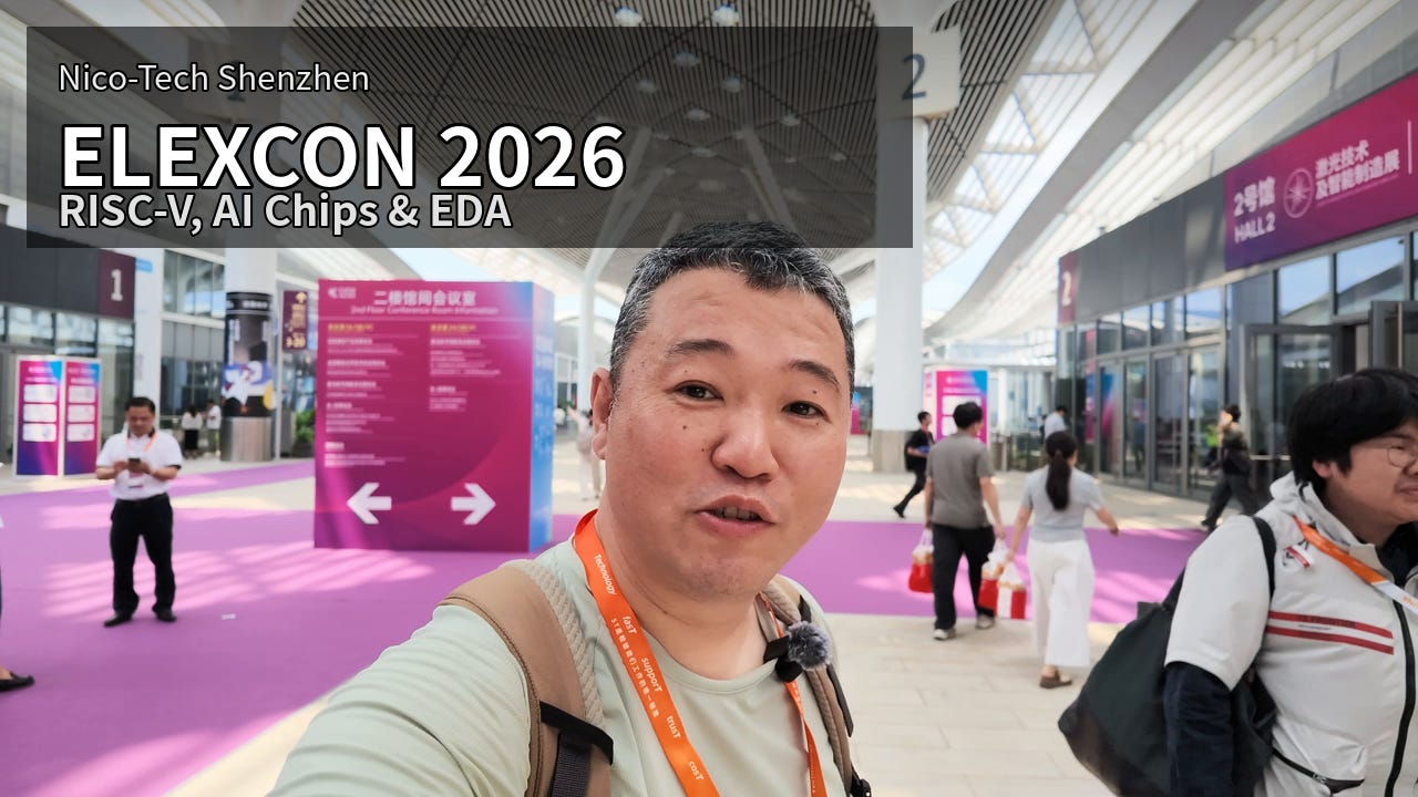
I spent a day walking through CIOE and elexcon 2026 at the Shenzhen World Exhibition & Convention Center in Bao’an. CIOE is one of the large optics and photonics exhibitions held in Shenzhen, covering cameras, lenses, displays, lasers, sensors, machine vision and the equipment built around them. At the same time, other halls were filled with semiconductor manufacturing, embedded systems and electronics-related exhibitions. I started in Hall 1 with optics and smart manufacturing, moved through the semiconductor manufacturing exhibition in Hall 14, and eventually reached elexcon in Hall 16.
The scale matters here. The Shenzhen exhibition center stretches from Hall 1 to Hall 18, and a very large part of it was occupied by electronics, manufacturing equipment and semiconductor-related companies. I have been living in Shenzhen and visiting Chinese electronics exhibitions for years, so the interesting part for me is no longer simply that there are many Chinese companies. What has changed is the range of industries represented and the degree of specialization inside each one.
▶ Watch from 00:00 — entering CIOE / elexcon 2026
▶ 04:40 — the scale of the Shenzhen exhibition center
For years, China’s semiconductor ambitions have usually been discussed through the language of localization, industrial policy, export controls, or US-China competition. Those issues are real, but they are not necessarily the most useful way to understand what is happening on an exhibition floor. What I saw this time was a growing number of companies doing business at different layers: manufacturing equipment, materials, chip design, finished semiconductors, development environments, and applications built on top of them.
That gradual thickening of the industrial stack was probably the most important thing I took away from the show.
The world’s factory is also a huge market for upgrading factories
Hall 1 was packed with companies working on cameras, lenses, CMOS sensors, image processing and visual inspection. Some companies make lenses or camera modules. Others integrate them into inspection systems. Nearby were machines for automated soldering, assembly and wire bonding. Large international vendors such as Keysight were present as well, so this was not a closed Chinese ecosystem.
Sunny Optical was particularly useful as an example of how wide the optical supply chain has become. Its displays included optical components for AR and XR glasses, small projection systems, RGB cameras and dToF depth sensors. These are not isolated technologies. They are pieces that eventually become smart glasses, machine-vision systems, robots or automated production equipment.
▶ 01:00 — cameras, optics and smart manufacturing
▶ 03:00 — automated inspection, soldering and assembly equipment
▶ 03:28 — Sunny Optical and AR / XR optics
China has an enormous number of factories, and those factories themselves are a market. When manufacturers automate inspection or improve quality control, they need cameras, sensors, image-processing chips, AI inference, controllers and software. A visual-inspection system alone involves optics, sensors, processors, software for classification, and the equipment company that integrates the whole thing into a production line.
This is one reason I think the phrase “the world’s factory” is often understood too narrowly. China is not only producing goods for the rest of the world. Its enormous manufacturing base also creates domestic demand for the technologies needed to upgrade those factories. Shenzhen’s machine-vision and smart-manufacturing companies have a very large customer base nearby.
The semiconductor ecosystem is expanding into equipment and materials
Hall 14 focused more directly on semiconductor manufacturing. Near the entrance was HDSC, a major Chinese state-owned semiconductor company, showing MCUs and applications including smart meters, display control and smart-home systems. Midea’s MR Semiconductor was also there. Midea is best known globally as a home-appliance manufacturer, but the group also owns KUKA and has industrial-robotics businesses, so its semiconductor development extends into motor control, high-current applications, industrial equipment and automotive electronics.
▶ 05:45 — entering the semiconductor manufacturing exhibition
▶ 05:58 — HDSC and Chinese MCUs
▶ 06:25 — Midea Group’s MR Semiconductor
Chinese semiconductor companies themselves are not new. What stood out more this time was the visibility of companies specializing in manufacturing equipment and materials. There were companies presenting composite materials and other specialized inputs with their own booths, talking directly with customers looking for those products.
Semiconductor materials and manufacturing equipment are areas where Japanese companies have historically been strong. Seeing Chinese suppliers at an exhibition does not mean they have suddenly reached the same technological level as the strongest Japanese, American or European companies. That is not the point. The important change is that there are now more domestic companies trying to supply parts of the stack that previously would have been imported, and there are also more customers at the exhibition actively looking for those suppliers.
▶ 12:10 — what I mean by greater “breadth and depth”
▶ 12:38 — semiconductor manufacturing equipment and materials
▶ 12:50 — from manufacturing and materials to design, chips and applications
Several years ago, I often heard the phrase “Chinese semiconductor localization” mainly as a government objective. Today, even though China still depends on foreign technologies and suppliers in many areas, it is easier to see a functioning commercial structure around that objective. There are companies for manufacturing, materials, design, finished chips and applications, and there are customers walking the same halls looking for them.
For me, this is more informative than asking whether semiconductor localization is “complete” or “not complete.” Industrial capabilities do not appear all at once. The more interesting question is how many layers of the stack can now support real companies, customers, engineers and transactions.
RISC-V is spreading across AI, servers and automotive systems
I spent a lot of time in the RISC-V area. What made it interesting was that the booths were not primarily explaining what RISC-V is. They were showing what they were building with it.
Suzhou-based C*CORE showed a RISC-V system combining CPU cores and an NPU, running Linux on a high-performance board. Other companies were presenting AI processors with 9 TOPS, 16 TOPS or more. There were also server-oriented systems using large multi-core RISC-V processors together with accelerator cards.
▶ 07:20 — entering the RISC-V area
▶ 07:31 — C*CORE: RISC-V plus AI
▶ 08:40 — discussing open-source AI chips at the booth
▶ 09:30 — RISC-V for servers
Shanghai-based CHIPV was showing automotive RISC-V. Its demo used RISC-V-based control hardware for functions such as the speedometer and indicators. This is a different market from the high-TOPS AI processors, but potentially just as important. Cars contain large numbers of controllers, so replacing or redesigning even relatively ordinary control functions around RISC-V can create a large market.
▶ 10:11 — automotive RISC-V in operation
Then there is Xuantie, developed within Alibaba’s T-Head ecosystem. What matters here is not only the CPU core. The booth represented IP, toolchains, programming environments and the surrounding development stack, from embedded applications up to higher-performance computing.
RISC-V is often discussed in terms of the openness of the instruction set, but companies cannot ship products with an instruction set alone. They need toolchains, operating systems, libraries, boards, debugging tools and engineering organizations that have experience actually using the architecture. What I saw at elexcon suggested that the Chinese RISC-V ecosystem is moving further into those implementation layers.
▶ 11:01 — Xuantie / T-Head and the broader development ecosystem
A Chinese FPGA company publishing more than 300 developer courses
Hall 16, where elexcon itself was located, was closer to the part of the electronics industry that I work with regularly: finished MCUs, development boards, FPGA platforms and embedded-development tools. Companies from Shenzhen and nearby Zhuhai were prominent, including Allwinner and Gowin.
At the Allwinner area, I saw development boards for AI cameras and a demo in which an Allwinner AI processor detected a person’s hand movements and used the recognition result to control a robotic arm. STM32 handled the control side while Allwinner silicon handled the AI recognition. This kind of mixed-vendor architecture is entirely normal in real product development and is a useful reminder that “Chinese semiconductor localization” does not mean every product suddenly becomes 100% Chinese.
▶ 11:53 — arriving at elexcon in Hall 16
▶ 14:33 — Allwinner
▶ 15:09 — hand recognition controlling a robotic arm
One company I found especially interesting was ALINX. The name naturally made me ask whether it was related to Xilinx. It is not an FPGA manufacturer. Instead, it builds development boards and application solutions around Xilinx — now AMD — FPGAs, including automotive applications. The booth showed boards based on Zynq and other devices, and the company also works with Chinese FPGA suppliers such as Fudan Microelectronics.
▶ 16:09 — ALINX and its FPGA / automotive solutions
▶ 16:32 — asking directly about the relationship with Xilinx
The part that caught my attention was not the number of boards. ALINX has published more than 300 online lessons explaining how to develop with FPGA platforms.
▶ 17:12 — ALINX’s 300+ online developer courses
This is closely related to my own research on the developer-centric approach in hardware businesses. Sophisticated semiconductors cannot create markets simply by existing. Customers need engineers who know how to use them. That requires development boards, examples, training materials, tutorials and support.
Structurally, this reminded me of the relationship between Espressif and companies such as M5Stack. The semiconductor company provides increasingly capable silicon, while another layer of companies makes that technology accessible to a much larger population of developers.
When people compare semiconductor industries, they often focus on fabrication processes, transistor density or benchmark performance. Those comparisons matter, but they miss another important layer: who makes the technology usable? Developer education, evaluation boards, toolchains, design services and communities are also parts of a semiconductor ecosystem.
At elexcon, I saw more companies treating that layer as a real business.
From a Tsinghua University research paper to a startup in four months
The booth where I spent the longest time was developing an AI-based chip-design tool. The system generates Verilog from prompts and uses multiple agents to move through design and testing step by step.
The company had even built a promotional game called “Understanding AI Chip Design,” which Professor Junichi Akita of Kanazawa University tried at the booth.
▶ 18:35 — AI generating Verilog for chip design
▶ 18:49 — Prof. Junichi Akita tries the AI chip-design game
During the conversation, I learned that the team had roots in Tsinghua University and was connected with the Yao Class. The project had originally started as academic research. According to the people at the booth, it began with a paper, the university encouraged them to turn it into a company, they received funding, and the company itself had been established only about four months earlier.
Despite that, they said they were already in discussions with around five companies.
▶ 18:59 — talking with the Tsinghua team
▶ 19:20 — how the multi-agent chip-design system works
▶ 20:21 — from one research paper to a company
▶ 20:34 — four months old and already talking with potential customers
This does not mean the technology is already commercially proven. A working exhibition demo, a publishable research result, a stable commercial EDA tool and a product that can be inserted into a semiconductor company’s real design flow are very different stages.
I asked Prof. Akita what he thought. His assessment was essentially that the objective and the technical approach were reasonable, but that there was no way to know how good the product really was without actually using it.
▶ 20:59 — Prof. Akita’s reaction after seeing the system
He also made another point that I think is important. Once a university has produced a paper and helped establish a company, the next stage depends on whether there are people willing to work extremely hard on the product for years. Academic success and company success require different kinds of persistence.
▶ 21:19 — what it takes for a research spinout to become a real company
The interesting part for me was therefore not “AI can now design chips.” We are much too early to make that claim from a trade-show demo. The interesting part was that a research topic around generative AI and chip design could produce a company, obtain institutional support, reach an industry exhibition, and begin talking to semiconductor customers within a very short period.
That is an ecosystem story as much as a technology story.
Huaqiangbei is only one layer of Shenzhen’s electronics industry now
Shenzhen Huaqiang Group was also exhibiting at elexcon. Outside China, Huaqiangbei is usually associated with the enormous electronics markets selling smartphone components, modules and gadgets. But Huaqiang Group’s businesses extend into semiconductor distribution, analog and power ICs, appliance design and IoT-product development. At the booth were smart cameras, routers and other products that could easily appear under somebody else’s consumer brand.
▶ 13:43 — Shenzhen Huaqiang Group at elexcon
Seeing Huaqiang-related companies in the same event as RISC-V CPU cores, FPGA development platforms, semiconductor materials and AI-based EDA makes it increasingly difficult to describe Shenzhen simply as a place where you can buy components in Huaqiangbei and quickly assemble a product.
That description was useful ten years ago, and part of it remains true. Shenzhen is still unusually good at connecting components, engineering and manufacturing quickly. But the technical layers around that capability have been expanding in both directions: deeper into materials, semiconductors and development tools, and upward into more complex applications and platforms.
When I first began writing regularly about Shenzhen, it was still useful to explain that Chinese companies made decisions quickly, built prototypes quickly, and had unusually close access to supply chains. I wrote versions of that story myself many years ago.
Today I am more interested in what happened after that.
What did those companies accumulate after ten more years of engineering? Which activities that used to be imported have become local industries? Where did developer ecosystems appear? Which university research groups produced companies? Which of those companies found customers?
By the final hour of the exhibition, the booths around semiconductor materials, RISC-V, FPGA and EDA were still busy. The subject matter has become more specialized, but there were still plenty of visitors talking with vendors.
▶ 21:54 — walking the exhibition in the final hour and reflecting on the change
This does not mean China has suddenly achieved complete semiconductor self-sufficiency, nor that every company on the floor has world-class technology. Many systems I saw still use AMD, Xilinx, STM32, SEGGER, Keysight and other international technologies and companies.
That mixture is precisely why I find the exhibition useful.
Industrial development is rarely a clean transition from “foreign” to “domestic.” What I saw was a gradual increase in the number of layers where Chinese companies can build businesses: materials, equipment, semiconductors, EDA, development platforms, engineering services and applications.
No single Chinese chip at elexcon suddenly changes the world. The more consequential change is that the surrounding industrial structure keeps getting denser.
That is why I keep going back to these exhibitions.
It is one of the easiest places to see the accumulation happening in physical form.
▶ 22:29 — closing thoughts from the exhibition
Watch the full field report on YouTube:
China’s semiconductor ecosystem on the ground — elexcon / CIOE 2026 in Shenzhen
English and Chinese subtitles are available on the video.